Semiconductor Devices Class 12 Exercise Question Answers Solutions Maharashtra Board
Balbharti Maharashtra State Board 12th Physics Textbook Solutions Chapter 16 Semiconductor Devices Textbook Exercise Questions and Answers.
Class 12 Physics Chapter 16 Exercise Solutions Maharashtra Board
Physics Class 12 Chapter 16 Exercise Solutions
1. Choose the correct option
i.
In a BJT, the largest current flow occurs
(A) in the emitter
(B) in the collector
(C) in the base
(D) through CB junction.
Answer:
(A) in the emitter
ii.
A series resistance is connected in the Zener diode circuit to
(A) properly reverse bias the Zener
(B) protect the Zener
(C) properly forward bias the Zener
(D) protect the load resistance.
Answer:
(A) properly reverse bias the Zener
![]()
iii.
An LED emits visible light when its
(A) junction is reverse biased
(B) depletion region widens
(C) holes and electrons recombine
(D) junction becomes hot.
Answer:
(C) holes and electrons recombine
iv.
Solar cell operates on the principle of
(A) diffusion
(B) recombination
(C) photovoltaic action
(D) carrier flow.
Answer:
(C) photovoltaic action
v.
A logic gate is an electronic circuit which
(A) makes logical decisions
(B) allows electron flow only in one direction
(C) works using binary algebra
(D) alternates between 0 and 1 value.
Answer:
(A) makes logical decisions
2 Answer in brief.
i.
Why is the base of a transistor made thin and is lightly doped?
Answer:
The base of a transistor is lightly doped than the emitter and is made narrow so that virtually all the electrons injected from the emitter (in an npn tran-sistor) diffuse right across the base to the collector junction without recombining with holes. That is, the base width is kept less than the recombination distance. Also, the emitter is much heavily doped than the base to improve emitter efficiency and common-base current gain a.
ii.
How is a Zener diode different than an ordinary diode?
Answer:
A Zener diode is heavily doped-the doping con-centrations for both p- and n-regions is greater than 1018 cm-3 while those of an ordinary diode are voltage (PIV) of an ordinary diode is higher than a Zener diode and the breakdown occurs by impact ionization (avalanche process). Their I-V characteristics are otherwise similar.
iii.
On which factors does the wavelength of light emitted by a LED depend?
Answer:
The intensity of the emitted light is directly propor-tional to the recombination rate and hence to the diode forward current. The colour of the light emitted by an LED depends on the compound semiconductor material used and its composition (and doping levels) as given below :
Table: Typical semiconductor materials and emitted colours of LEDs
| Material | Emitted colour(s) |
| Gallium arsenide (GaAs), Indium gallium arsenide phosphide (InGaAsP) | Infrared |
| Aluminum gallium arsenide (AlGaAs) | Deep red, also IR laser |
| Indium gallium phosphide (InGaP) | Red |
| Gallium arsenide phosphide (GaAsP), aluminum indium gallium phosphide (AlInGaP) | Orange, red or yellow |
| Gallium phosphide (GaP) | Green or yellow |
| Aluminium gallium phosphide (AlGaP), zinc selenide (ZnSe), zinc selenide telluride (ZnSeTe), nitrogen impregnated gallium phosphide (GaP:N) | Green |
| Indium gallium nitride (InGaN), gallium nitride (GaN), sine sulphide (ZnS) | Blue and violet Longer wave lengths (green and yellow) are obtained by increasing the indium (In) content. Phosphor encapsulation produce white light. |
| Aluminium gallium nitride (AlGaN)
| Ultraviolet |
iv.
Why should a photodiode be operated in reverse biased mode?
Answer:
A photodiode is operated in a reverse biased mode because as photodetector or photosensor, it must conduct only when radiation is incident on it. In the reverse biased mode, the dark current for zero illumination is negligibly small—of the order of few picoamperes to nanoamperes. But when illuminated, the photocurrent is several orders of magnitude greater.
v.
State the principle and uses of a solar Cell.
Answer:
A solar cell is an unbiased pn-junction that converts the energy of sunlight directly into electricity with a high conversion efficiency.
Principle : A solar cell works on the photovoltaic effect in which an emf is produced between the two layers of a pn-junction as a result of irradiation.
![]()
Question 3.
Draw the circuit diagram of a half wave rectifier. Explain its working. What is the frequency of ripple in its output?
Answer:
A device or a circuit which rectifies only one-half of each. cycle of an alternating voltage is called a half-wave rectifier.
Electric circuit : The alternating voltage to be rectified is applied across the primary coil (P1P2) of a transformer. The secondary coil (S1S2) of the transformer is connected in series with the junction diode and a load resistance RL, as shown in below figure. The alternating voltage across the secondary coil is the ac input voltage Vi. The dc voltage across the load resistance is called the output voltage V0.
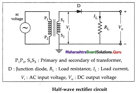
Working : Due to the alternating voltage Vi, the p-region of the diode becomes alternatively positive and negative with respect to the n-region.
During the half-cycle when the p-region is positive, the diode is forward biased and conducts. A current IL passes through the load resistance RL in the direction shown.
During the next half cycle, when the p-region is negative, the diode is reverse biased and the forward current drops to zero.
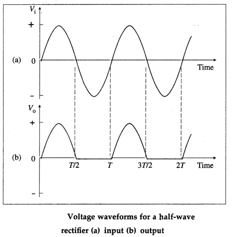
Thus, the diode conducts only during one-half of the input cycle and thus acts as a half-wave rectifier. The intermittent output voltage V0 has a fixed polarity but changes periodically with time between zero and a maximum value. IL is unidirectional. Above figure shows the input and output voltage waveforms.
The pulsating dc output voltage of a half-wave rectifier has the same frequency as the input.
Question 4.
Why do we need filters in a power supply?
Answer:
A rectifier-half-wave or full-wave – outputs a pul-sating dc which is not directly usable in most electronic circuits. These circuits require something closer to pure dc as produced by batteries. Unlike pure dc waveform of a battery, a rectifier output has an ac ripple riding on a dc waveform.
The circuit used in a dc power supply to remove the ripple is called a filter. A filter circuit can produce a very smooth waveform that approximates the waveform produced by a battery. The most common technique used for filtering is a capacitor connected across the output of a rectifier.
Question 5.
Draw a neat diagram of a full wave rectifier and explain it’s working.
Answer:
A device or a circuit which rectifies both halves of each cycle of an alternating voltage is called a full-wave rectifier.
Electric circuit : The alternating voltage to be rectified is applied across the primary coil (P1P2) of a transformer with a centre-tapped secondary coil (S1S2). The terminals and S2 of the secondary are connected to the two p-regions of two junction diodes D1 and D2, respectively. The centre-tap T is connected to the ground. The load resistance RL is connected across the common n-regions and the
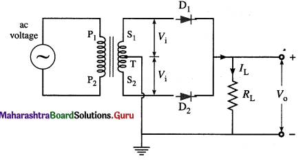
P1P2, S1S2 : Primary and secondary of transformer,
T : Centre-tap on secondary; D1 D2 : Junction diodes,
RL : Load resistance, IL : Load current,
Vi: AC input voltage, V0 : DC output voltage
Above Figure : Full-wave rectifier circuit
Working : During one half cycle of the input, terminal S1 of the secondary is positive while S2 is negative with respect to the ground (the centre-tap T). During this half cycle, diode D1 is forward biased and conducts, while diode D2 is reverse biased and does not conduct. The direction of current ZL through RL is in the sense shown.
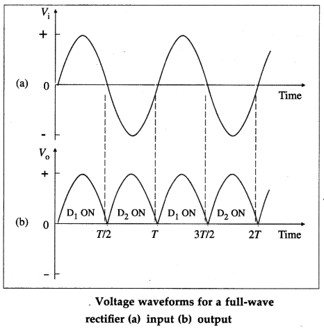
During the next half cycle of the input voltage, S2 becomes positive while S, is negative with respect to T. Diode D2 now conducts sending a current IL through RL in the same sense as before. Dt now does not conduct. Thus, the current through RL flows in the same direction, i.e., it is unidirectional, for both halves or the full-wave of the input. This is called full-wave rectification.
The output voltage has a fixed polarity but varies periodically with time between zero and a maximum value. Above figure shows the input and output voltage waveforms. The pulsating dc output voltage of a full-wave rectifier has twice frequency of the input.
Question 6.
Explain how a Zener diode maintains constant voltage across a load.
Answer:
Principle : In the breakdown region of a Zener diode, for widely changing Zener current, the voltage across the Zener diode remains almost constant.
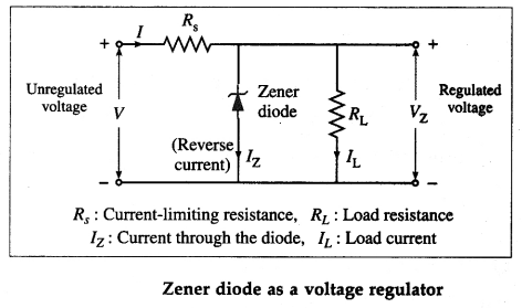
Electric circuit : The circuit for regulating or stabilizing the voltage across a load resistance RL against change in load current and supply voltage is shown in above figure. The Zener diode is connected parallel to load Rh such that the current through the Zener diode is from the n to p region. The series resistance Rs limits the current through the diode below the maximum rated value.
From the circuit, I = IZ + IL and V = IRs + VZ
= (IZ + IL)Rs + VZ
Working: When the input unregulated dc voltage V across the Zener diode is greater than the Zener voltage VZ in magnitude, the diode works in the Zener breakdown region. The voltage across the diode and load Rh is then VZ. The corresponding current in the diode is IZ.
As the load current (I) or supply voltage (V) changes, the diode current (7Z) adjusts itself at constant VZ. The excess voltage V-VZappears across the series resistance Rs.
For constant supply voltage, the supply current I and the voltage drop across Rs remain constant. If the diode is within its regulating range, an increase in load current is accompanied by a decrease in Iz at constant VZ.
Since the voltage across RL remains constant at VZ, the Zener diode acts as a voltage stabilizer or voltage regulator.
![]()
Question 7.
Explain the forward and the reverse characteristic of a Zener diode.
Answer:
The forward bias region of a Zener diode is identical to that of a regular diode. There is forward current only after the barrier potential of the pn- junction is overcome. Beyond this threshold or cut in voltage, there is an exponential upward swing.
The typical forward voltage at room temperature with a current of around 1 mA is around 0.6 V.
In the reverse bias condition the Zener diode is an open circuit and only a small reverse saturation current flows as shown with change of scale. At the reverse breakdown voltage there is an abrupt rapid increase in the current-the knee is very sharp, followed by an almost vertical increase in current. The voltage across the Zener diode in the breakdown region is very nearly constant with only a small increase in voltage with increasing current. There is a minimum Zener current, IZ (min), that places the operating point in the desired breakdown region. At some high current level, IZM, the power dissipation of the diode becomes excessive beyond which the diode can be damaged.
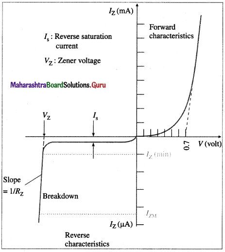
Zener diode characteristics
The I-V characteristics of a Zener diode is not totally vertical in the breakdown region. This means that for slight changes in current, there will be a small change in the voltage across the diode. The voltage change for a given change in current is the resistance RZ of the Zener diode.
Question 8.
Explain the working of a LED.
Answer:
Working :
An LED is forward-biased with about 1.2 V to 3.6 V at 12 mA to 20 mA. Majority carriers electrons from n-type layer and holes from p-type layer are injected into the active layer. Electrons cross the junction into the p-layer. In the active p-layer, some of these excess minority carriers electrons, recombine radiatively with majority carriers, holes, thereby emitting photons. The resulting photon has an energy approximately equal to the bandgap of the active layer material. Modifying the bandgap of the active layer creates photons of diferent energies.
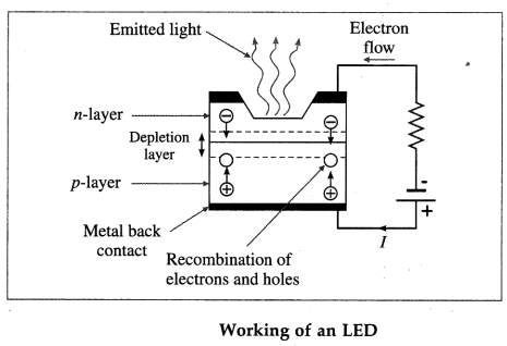
In the energy band diagram this recombination is equivalent to a transition of the electron from a higher energy state in the conduction band to a lower energy state in the valence band. The energy difference is emitted as a photon of energy hv.
[Note : The photons originate primarily in the p-side of the junction which has a bandgap EGp narrower than that of the n-side, EGn. Thus, with hv < EGn, the photons are emitted through the wide-bandgap n-region with essentially no absorption.]
Question 9.
Explain the construction and working of solar cell.
Answer:
Construction :
A simple pn-junction solar cell con-sists of a p-type semiconductor substrate backed with a metal electrode back contact. A thin n-layer (less than 2.5 pm, for silicon) is grown over the p-type substrate by doping with suitable donor impurity. Metal finger electrodes are prepared on top of the n-layer so that there is enough space between the fingers for sunlight to reach the n-layer and, subsequently, the underlying pn-junction.
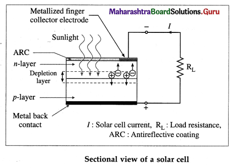
Working : When exposed to sunlight, the absorption of incident radiation (in the range near-UV to infrared) creates electron-hole pairs in and near the depletion layer.
Consider light of frequency v incident on the pn-junction such that the incident photon energy hv is greater than the band gap energy EG of the semiconductor. The photons excite electrons from the valence band to the conduction band, leaving vacancies or holes in the valence band, thus generating electron-hole pairs.
The photogenerated electrons and holes move towards the n side and p side, respectively. If no external load is connected, these photogenerated charges get collected at the two sides of the junction and give rise to a forward photovoltage. In a closed- circuit, a current I passes through the external load as long as the solar cell is exposed to sunlight.
A solar cell module consists of several solar cells connected in series for a higher voltage output. For outdoor use with higher power output, these modules are connected in different series and parallel combinations to form a solar cell array.
[Note : Currently most of the crystalline solar cells are p-type as described above. This is because of a lower cost of production of p-type. But performance wise, n-type solar cells (a thin p-layer over an n-type substrate by doping with suitable acceptor impurity) can give much better efficiency compared to p-type solar cells.]
![]()
Question 10.
Explain the principle of operation of a photodiode.
Answer:
Construction:
A photodiode consists of an n-type silicon substrate with a metal electrode back contact. A thin p-type layer is grown over the n-type substrate by diffusing a suitable acceptor dopant.
The area of the p-layer defines the photodiode active area. An ohmic contact pad is deposited on the active area. The rest of the active area is left open with a protective antireflective coating of silicon nitride to minimize the loss of photons. The nonactive area is covered with an insulating opaque SiO2 coating.
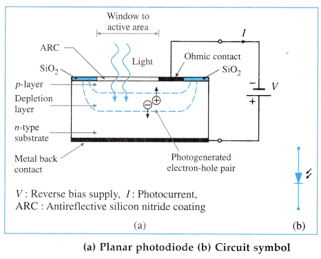
Depending on the required spectral sensitivity, i.e., the operating wavelength range, typical photodiode materials are silicon, germanium, indium gallium arsenide phosphide (InGaAsP) and indium gallium arsenide (InGaAs), of which silicon is the cheapest while the last two are expensive.
Working : The band gap energy of silicon is EG = 1.12 eV at room temperature. Thus, photons or particles with energies greater than or equal to 1.12 eV, which corresponds to 110 nm, can transfer electrons from the valence band into the conduction band.
A photodiode is operated in the reverse bias mode which results in a wider depletion region. When operated in the dark (zero illumination), there is a reverse saturation current due solely to the thermally generated minority charge carriers. This is called the dark current. Depending on the minority carrier concentrations, the dark current in an Si photodiode may range from 5 pA to 10 nA.
When exposed to radiation of energy hv ≥ EG (in the range near-UV to near-IR), electron-hole pairs are created in the depletion region. The electric field in the depletion layer accelerates these photogenerated electrons and holes towards the n side and p side, respectively, constituting a photocurrent l in the external circuit from the p side to the n side. Due to the photogeneration, more charge carriers are available for conduction and the reverse current is increased. The photocurrent is directly propor-tional to the intensity of the incident light. It is independent of the reverse bias voltage.
[Notes : Typical photodiode materials are :
(1) silicon (Si) : low dark current, high speed, good sensitivity between ~ 400 nm and 1000 run (best around 800 nm-900 nm)
(2) germanium (Ge) : high dark current, slow speed, good sensitivity between ~ 900 nm and 1600 nm (best around 1400 nm-1500 nm)
(3) indium gallium arsenide phosphide (InGaAsP) : expensive, low dark current, high speed, good sensitivity between ~ 1000 nm and 1350 nm (best around 1100 nm- 1300 nm)
(4) indium gallium arsenide (InGaAs): expensive, low dark current, high speed, good sensitivity between ~ 900 nm and 1700 nm (best around 1300 nm-1600 nm],
Question 11.
What do you mean by a logic gate, a truth table and a Boolean expression?
Answer:
A logic gate is a basic switching circuit used in digital circuits that determines when an input pulse can pass through to the output. It generates a single output from one or more inputs.
Explanation/Uses :
Any digital computation process consists in performing a sequence of arithmetical operations on the data of the problem. At each stage in the computation, the nature of the operation to be performed is decided partly by the pre-determined program and partly by the outcome of earlier stages in the process. We therefore need switches with multiple inputs to perform logical operations, i.e., the outputs of these switches are determined in specified ways by the condition (binary state) of their inputs. These arrangements are known as logic gates, and mostly they are extension of a simple transistor switch.
(1) Boolean expression : An equation expressing a logical compound statement in Boolean algebra is called a Boolean expression. A Boolean expression for a logic gate expresses the relation between input(s) and output of a logic gate.
(2) Truth table : The table which shows the truth values of a Boolean expression for a logic gate for all possible combinations of its inputs is called the truth table of logic gate.
The truth table contains one row for each input combination. Since a logical variable can assume only two possible values, 0 and 1, there are 2N combinations of N inputs so that the table has 2N rows.
[Note : Boolean algebra is a form of symbolic logic developed in 1847 by George Boole (1815-64) British mathematician.]
![]()
Question 12.
What is logic gate? Write down the truth table and Boolean expression for ‘AND’ gate.
Answer:
A logic gate is a basic switching circuit used in digital circuits that determines when an input pulse can pass through to the output. It generates a single output from one or more inputs.
The AND gate : It is a circuit with two or more inputs and one output in which the output signal is HIGH if and only if all the inputs are HIGH simultaneously.
The AND operation represents a logical multiplication.
Below figure shows the 2-input AND gate logic symbol and the Boolean expression and the truth table for the AND function.
Logic symbol:
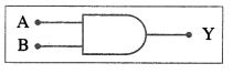
Truth table:
Boolean expression:
Y = A ∙ B
Question 13.
What are the uses of logic gates? Why is a NOT gate known as an inverter?
Answer:
Explanation/Uses :
Any digital computation process consists in performing a sequence of arithmetical operations on the data of the problem. At each stage in the computation, the nature of the operation to be performed is decided partly by the pre-determined program and partly by the outcome of earlier stages in the process. We therefore need switches with multiple inputs to perform logical operations, i.e., the outputs of these switches are determined in specified ways by the condition (binary state) of their inputs. These arrangements are known as logic gates, and mostly they are extension of a simple transistor switch.
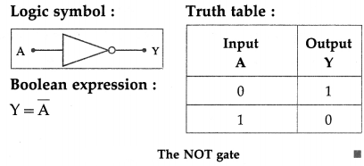
The NOT gate or INVERTER : It is a circuit with one input whose output is HIGH if the input is LOW and vice versa.
The NOT operation outputs an inverted version of the input. Hence, a NOT gate is also known as an INVERTER.
The small invert bubble on the output side of the inverter logic symbol, below figure and the over bar (–) in the Boolean expression represent the invert function.
Question 14.
Write the Boolean expression for (i) OR gate, (ii) AND gate, and (iii) NAND Gate.
Answer:
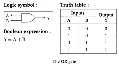
(i) The OR gate : It is a circuit with two or more inputs and one output in which the output signal is HIGH if any one or more of the inputs is HIGH.
The OR operation represents a logical addition.
Below figure shows the 2-input OR gate logic sym-bol, and the Boolean expression and the truth table for the OR function.
(ii) The AND gate : It is a circuit with two or more inputs and one output in which the output signal is HIGH if and only if all the inputs are HIGH simultaneously.
The AND operation represents a logical multiplication.
Below figure shows the 2-input AND gate logic symbol and the Boolean expression and the truth table for the AND function.
Logic symbol:
Truth table:
Boolean expression:
Y = A ∙ B
(iii) The NAND gate : It is a circuit with two or more inputs and one output, whose output is HIGH if any one or more of the inputs is LOW; the output is LOW if all the inputs are HIGH.
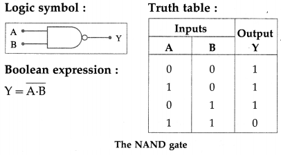
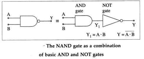
The NAND gate is a combination of an AND gate followed by a NOT gate so that the truth table of the NAND function is obtained by inverting the outputs of the AND gate.
Question 15.
Why is the emitter, the base and the collector of a BJT doped differently?
Answer:
A BJT being a bipolar device, both electrons and holes participate in the conduction process. Under the forward-biased condition, the majority carriers injected from the emitter into the base constitute the largest current component in a BJT. For these carriers to diffuse across the base region with t negligible recombination and reach the collector junction, these must overwhelm the majority carriers of opposite charge in the base. The total emitter current has two components, that due to majority carriers in the emitter and that due to minority carriers diffused from base into emitter. The ratio of the current component due to the injected majority carriers from the emitter to the total emitter current is a measure of the emitter efficiency. To improve the emitter efficiency and the common-base current gain (a), it can be shown that’ the emitter should be much heavily doped than the base.
Also, the base width is a function of the base- collector voltage. A low doping level of the collector increases the size of the depletion region. This increases the maximum collector-base voltage and reduces the base width. Further, the large depletion region at the collector-base junction-extending mainly into the collector-corresponds to a smaller electric field and avoids avalanche breakdown of the reverse-biased collector-base junction.
[Note : Effective dopant concentrations of (a) npn transistor (b) pnp transistor are shown below.
The base doping is less than the emitter doping but greater than the collector doping. Contrary to the impression stressed in the Board’s and NCERT textbooks, collector doping is typically an order of magnitude lower than base doping. {Ref. : Semiconductor Devices Physics and Technology (3rd Edition), Simon M. Sze and M. K. Lee, p. 125}]
Question 16.
Which method of biasing is used for operating transistor as an amplifier?
Answer:
For use as an amplifier, the transistor should be in active mode. Therefore, the emitter-base junction is forward biased and the collector-base junction is reverse biased. Also, an amplifier uses an emitter bias rather than a base bias.
![]()
Question 17.
Define α and β. Derive the relation between then.
Answer:
The dc common-base current ratio or current gain (αdc) is defined as the ratio of the collector current to emitter current.
αdc = \(\frac{I_{C}}{I_{\mathrm{E}}}\)
The dc common-emitter current ratio or current gain (βdc) is defined as the ratio of the collector current to base current.
βdc = \(\frac{I_{C}}{I_{B}}\)
Since the emitter current IE = IB + IC
\(\frac{I_{\mathrm{E}}}{I_{C}}=\frac{I_{\mathrm{B}}}{I_{\mathrm{C}}}+1\)
∴ \(\frac{1}{\alpha_{\mathrm{dc}}}=\frac{1}{\beta_{\mathrm{dc}}}+1\)
Therefore, the common-base current gain in terms of the common-emitter current gain is
αdc = \(\frac{\beta_{\mathrm{dc}}}{1+\beta_{\mathrm{dc}}}\)
and the common-emitter current gain in terms of the common-base current gain is
βdc = \(\frac{\alpha_{\mathrm{dc}}}{1-\alpha_{\mathrm{dc}}}\)
For a transistor, αdc is close to but always less than 1 (about 0.92 to 0.98) and βdc ranges from 20 to 200 for most general purpose transistors.
Question 18.
The common-base DC current gain of a transistor is 0.967. If the emitter current is 10mA. What is the value of base current?
Answer:
Data : αdc = 0.967, IE = 10 mA
αdc = \(\frac{I_{C}}{I_{\mathrm{E}}}\) and IE = IB + IC
The collector current,
IC = αdcIE = 0.967 × 10 = 9.67 mA
Therefore, the base current,
IB = IE – IC = 10 – 9.67 = 0.33 mA
Question 19.
In a comman-base connection, a certain transistor has an emitter current of 10mA and collector current of 9.8 mA. Calculate the value of the base current.
Answer:
DATA : IE = 10 mA, IC = 9.8 mA
IE = IB + IC
Therefore, the base current,
IB = IE – IC – 10 – 9.8 = 0.2 mA
Question 20.
In a common-base connection, the emitter current is 6.28mA and collector current is 6.20 mA. Determine the common base DC current gain.
Answer:
Data : IE = 6.28 mA, IC = 6.20 mA
αdc = \(\frac{I_{C}}{I_{\mathrm{E}}}\) and βdc = \(\frac{I_{\mathrm{C}}}{I_{\mathrm{B}}}=\frac{\alpha_{\mathrm{dc}}}{1-\alpha_{\mathrm{dc}}}\)
Common-emitter current gain, αdc = \(\frac{6.20}{6.28}\) = 0.9873
Therefore, common-base current gain,
βdc = \(\frac{0.9873}{1-0.9873}=\frac{0.9873}{0.0127}\) = 77.74
OR
IE = IB + IC
∴ IB = IE – IC = 6.28 – 6.20 = 0.08 mA
∴ βdc = \(\frac{6.20}{0.08}\) = 77.5
[Note : The answer given in the textbook obviously refers to the common-emitter current gain.]
12th Physics Digest Chapter 16 Semiconductor Devices Intext Questions and Answers
Remember this (Textbook Page No. 346)
Question 1.
A full wave rectifier utilises both half cycles of AC input voltage to produce the DC output.
Answer:
A half-wave rectifier rectifies only one half of each cycle of the input ac wave while a full-wave rectifier rectifies both the halves. Hence the pulsating dc output voltage of a half-wave rectifier has the same frequency as the input but that of a full-wave rectifier has double the frequency of the ac input.
Do you know (Textbook Page No. 346)
Question 1.
The maximum efficiency of a full wave rectifier is 81.2% and the maximum efficiency of a half wave rectifier is 40.6%. It is observed that the maximum efficiency of a full wave rectifier is twice that of half wave rectifier.
Answer:
The ratio of dc power obtained at the output to the applied input ac power is known as rectifier efficiency. A half-wave rectifier can convert maximum 40.6% of ac power into dc power, and the remaining power of 59.4% is lost in the rectifier circuit. In fact, 50% power in the negative half cycle is not converted and the remaining 9.4% is lost in the circuit. Hence, a half wave rectifier efficiency is 40.6%. The maximum efficiency of a full-wave rectifier is 81.2%, i.e., twice that of a half-wave rectifier.
Do you know (Textbook Page No. 349)
Question 1.
The voltage stabilization is effective when there is a minimum Zener current. The Zener diode must be always operated within its breakdown region when there is a load connected in the circuit. Similarly, the supply voltage Vs must be greater than Vz.
Answer:
A Zener diode is operated in the breakdown region. There is a minimum Zener current, Iz, that places the desired operating point in the breakdown region. There is a maximum Zener current, IzM, at which the power dissipation drives the junction temperature to the maximum allowed. Beyond that current the diode can be damaged. Hence, the supply voltage must be greater than Vz and the current-limiting resistor must limit the diode current to less than the rated maxi mum, IzM.
Remember this (Textbook Page No. 350)
Question 1.
Zener effect occurs only if the diode is heavily doped, because when the depletion layer is thin, breakdown occurs at low reverse voltage and the field strength will be approximately 3 × 10⁷ V/m. It causes an increase in the flow of free carriers and increase in the reverse current.
Answer:
Zener breakdown occurs only in heavily doped pn junctions (doping concentrations for both p- and n-regions greater than 1018 cm3) and can take place only if the electric field in the depletion region of the reverse-biased junction is very high. It is found that the critical field at which tunneling becomes probable, i.e., at which Zener breakdown commences, is approximately 106 V/cm. [“internal Field Emissiot at Narrow Silicon and Germanium PN-Junctions,” Phys. Rev., 118, 425 (1960).]
Can you tell (Textbook Page No. 350)
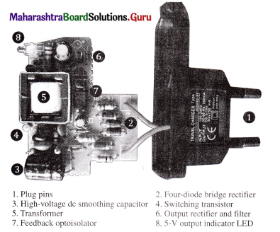
Question 1.
How does a cell phone charger produce a voltage of 5.0 V form the line voltage of 230V?
Answer:
A phone charger is usually a 5 V power supply. A 4-diode bridge input rectifier rectifies the ac mains voltage a provide a high voltage dc. A transistor chopper switches this on and off at high frequency. This stage is required because this high frequency allows the transformer to be smaller, lighter and much lower in cost.
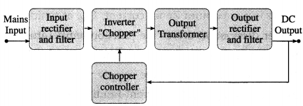
A small transformer steps this down to a low voltage high-frequency ac. An output rectifier and filter convert this to low-voltage (5 V) dc and smooths out the ripple. A chopper controller provides a feedback to the chopper through an optoisohitor and adjusts the chopping cycle to maintain the output voltage at 5 V.
Question 2.
Why is a resistance connected in series with a Zener diode when used in a circuit?
Answer:
The I-V characteristics in the breakdown region of a Zener diode is almost vertical. That is, the current IZ can rapidly increase at constant VZ. To prevent damage due to excessive heating, the Zener current should not exceed the rated maximum current, IZM. Hence, a current-limiting resistor Rs is connected in series with the diode.
IZ and the power dissipated in the Zener diode will be large for I L = 0 (no-load condition) or when IL is less than the rated maximum (when Rs is small and RL is large). The current-limiting resistor Rs is so chosen that the Zener current does not exceed the rated maximum reverse current, IZM when there is no load or when the load is very high.
The rated maximum power of a Zener diode is
PZM = IZM = VZ
At n-load condition, the current through R is I = IZM and the voltage drop across it is V – VZ, where V is the unregulated source voltage. The diode current will be maximum when V is maxi mum at Vmax and I = IZM. Then, the minimum value of the series resistance should be
Rs, min = \(\frac{V_{\max }-V_{\mathrm{Z}}}{I_{\mathrm{ZM}}}\)
Question 3.
The voltage across a Zener diode does not remain strictly constant with the changes in the Zener current. This is due to RZ, the Zener impedance, or the internal resistance of the Zener diode. RZ acts like a small resistance in series with the Zener. Changes in IZ cause small changes in VZ .
Answer:
The I-V characteristics of a Zener diode in the breakdown region is not strictly vertical. Its slope is 1/RZ, where RZ is the Zener impedance.
Can you know (Textbook Page No. 354)
Question 1.
What is the difference between a photo diode and a solar cell?
Answer:
Both are semiconductor photovoltaic devices. A photodiode is a reverse-biased pn-junction diode while a solar cell is an unbiased pn-junction diode. Photod iodes, however, are optimized for light detection while solar cells are optimized for energy conversion efficiency.
Question 2.
When the intensity of light incident on a photo diode increases, how is the reverse current affected?
Answer:
The photocurrent increases linearly with increasing illuminance, limited by the power dissipation of the photodiode.
Do you know (Textbook Page No. 355)
Question 1.
LED junction does not actually emit that much light so the epoxy resin body is constructed in such a way that the photons emitted by the junction are reflected away from the surrounding substrate base to which the diode is attached and are focused upwards through the domed top of the LED, which itself acts like a lens concentrating the light. This is why the emitted light appears to be brightest at the top of the LED.
Answer:
The pn-junction of an LED is encased in a transparent, hard plastic (epoxy resin), not only for shock protection but also for enhancing the brightness in one direction. Light emitted by the pn-junction is not directional. The hemispherical epoxy lens focuses the light in the direction of the hemispherical part. This is why the emitted light appears to be brightest at the top of the LED.
Question 2.
The current rating of LED is of a few tens of milli-amps. Hence it is necessary to connect a high resistance in series with it. The forward voltage drop of an LED is much larger than an ordinary diode and is around 1.5 to 3.5 volts.
Answer:
Most common LEDs require a forward operating voltage of between approximately 1.2 V (for a standard red LED) to 3.6 V (for a blue LED) with a forward current rating of about 10 mA to 30 mA, with 12 mA to 20 mA being the most common range. Like any diode, the forward current is approximately an exponential function of voltage and the forward resistance is very small. A small voltage change may result in a large change in current. If the current exceeds the rated maximum, an LED may overheat and get destroyed. LEDs are current driven devices and a current-limiting series resistor is required to prevent burning up the LED.
Do you know (Textbook Page No. 356)
Question 1.
White Light LEDs or White LED Lamps:
Shuji Nakamura, a Japanese – born American electronic engineer invented the blue LED. He was awarded the Nobel prize for physics for 2014. He was also awarded the global energy prize in the year 2015. His invention of blue LED made the fabrication of white LED possible.
LED lamps, bulbs, street lighting are becoming very popular these days because of the very high efficiency of LEDs in terms of light output per unit input power(in milliWatts), as compared to the incandescent bulbs. So for general purpose lightings, white light is preferred.
Commercially available white LEDs are normally manufactured by using the technique of wavelength conversion. It is a process which partly or completely converts the radiation of a LED into white light. There are many ways of wavelength conversion. One of these methods uses blue LED and yellow phosphor. In this method of wavelength conversion, a LED which emits blue colour is used to excite a yellow colour phosphor. This results in the emission of yellow and blue light and this mixture of blue and yellow light gives the appearance of white light. This method is the least expensive method for producing white light.
Answer:
The all important blue LEDs
The development of LEDs has made more efficient light sources possible. Creating white light that can be used for lighting requires a combination of red, green and blue light. Blue LEDs proved to be much more difficult to create than red and green LEDs. During the 1980s and 1990s Isamu Akasaki, Hiroshi Amano, and Shuji Nakamura successfully used the difficult-to-handle semiconductor gallium nitride to create efficient blue LEDs. Isamu Akasaki is known for invent ing the bright gallium nitride (CaN) pn-junction blue LED in 1989 and subsequently the high-brightness CaN blue LED.
Using blue LEDs, highly efficient white light sources. became possible by converting part of the blue light emitted from an LED to yellow using a phosphor. To the human eye, the combination of blue and yellow light is perceived as white. A white LED can be created by embedding phosphors in the plastic cap which surrounds a blue LED. Higher quality white light can also be created by mixing blue light with other colors as well, including red and green
Isamu Akasaki, together with Shuji Nakamura and Hiroshi Amano, received the 2014 Nobel Prize in Physics for the invention of efficient blue light-emitting diodes which has enabled bright and energy saving white light sources.
Use your brain power (Textbook Page No. 357)
Question 1.
What would happen if both junctions of a BJT are forward biased or reverse biased?
Answer:
A BJT has four regimes of operation, depending on the four combinations of the applied biases (voltage polarities) to the emitter-base junction and the collector-base junction, as shown in the following table; ‘F’ and ‘R’ indicate forward bias and reverse bias, respectively.
Remember This (Textbook Page No. 358)
Question 1.
The lightly doped, thin base region sandwiched between the heavily doped emitter region and the intermediate doped collector region plays a crucial role in the transistor action.
Answer:
If the two junctions in a BJT are physically close compared with the minority carrier diffusion length (i.e., the distance within which recombination will take place), the careers injected from the emitter can diffuse through the base to reach the base-collector junction. The narrow width of the base is thus crucial for transistor action.
Use your brain power (Textbook Page No. 361)
Question 1.
If a transistor amplifies power, explain why it is not used to generate power.
The term ‘amplification’ is used as an abstraction of the transistor properties so that we have few equations which are useful for a large number of practical problems. Transistors use a small power to control a power supply which can output a huge power. The large output comes from the power supply, while the input signal valves the transistor on and off. The increased power comes from the power supply so that a transistor does not violate the law of conservation of energy.
Maharashtra State Board Class 12 Textbook Solutions
- Current Electricity Class 12 Physics Textbook Solutions
- Magnetic Fields due to Electric Current Class 12 Physics Textbook Solutions
- Magnetic Materials Class 12 Physics Textbook Solutions
- Electromagnetic Induction Class 12 Physics Textbook Solutions
- AC Circuits Class 12 Physics Textbook Solutions
- Dual Nature of Radiation and Matter Class 12 Physics Textbook Solutions
- Structure of Atoms and Nuclei Class 12 Physics Textbook Solutions
- Semiconductor Devices Class 12 Physics Textbook Solutions